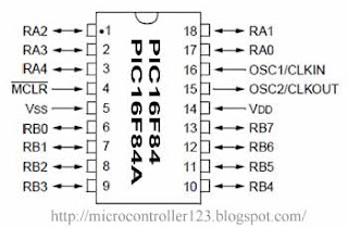
The given diagram showing the pin-outs of the PIC 16F84. I will go through each pin, explaining what each is used for. Microchip manufacture a series of microcontrollers called PIC. There are many different flavours available, some basic low memory types, going right up through to ones that have Analogue - To- Digital converters and even PWM built in. I am going to concentrate on the 16F84 PIC. Once you have learnt how to program one type of PIC, learning the rest is easy.
RA0 To RA4 : RA is a bidirectional port. That is, it can be configured as an input or an output. The number following RA is the bit number (0 to 4). So, we have one 5-bit directional port where each bit can be configured as Input or Output.
RB0 To RB7 : RB is a second bidirectional port. It behaves in exactly the same way as RA, except there are 8 - bits involved.
VSS And VDD : These are the power supply pins. VDD is the positive supply, and VSS is the negative supply, or 0V. The maximum supply voltage that you can use is 6V, and the minimum is 2V
OSC1/CLK IN And OSC2/CLKOUT : These pins is where we connect an external clock, so that the microcontroller has some kind of timing.
MCLR : This pin is used to erase the memory locations inside the PIC (i.e. when we want to re-program it). In normal use it is connected to the positive supply rail.
INT : This is an input pin which can be monitored. If the pin goes high, we can cause the program to restart, stop or any other single function we desire. We won't be using this one much.
T0CK1 : This is another clock input, which operates an internal timer. It operates in isolation to the main clock. Again, we won't be using this one much either.

No comments:
Post a Comment